[ Instrument Network Instrument Development ] In recent years, transient electronics has received more and more attention. Transient electronics can degrade themselves into the environment after completing specific preset functions, thereby avoiding the difficulties of handling and recycling e-waste and the environmental pollution caused by improper handling. Although it is currently feasible to prepare transient electronic devices on a water-soluble substrate by a transfer method, this method has a low yield, a limited circuit complexity, and is difficult to prepare on a large scale.
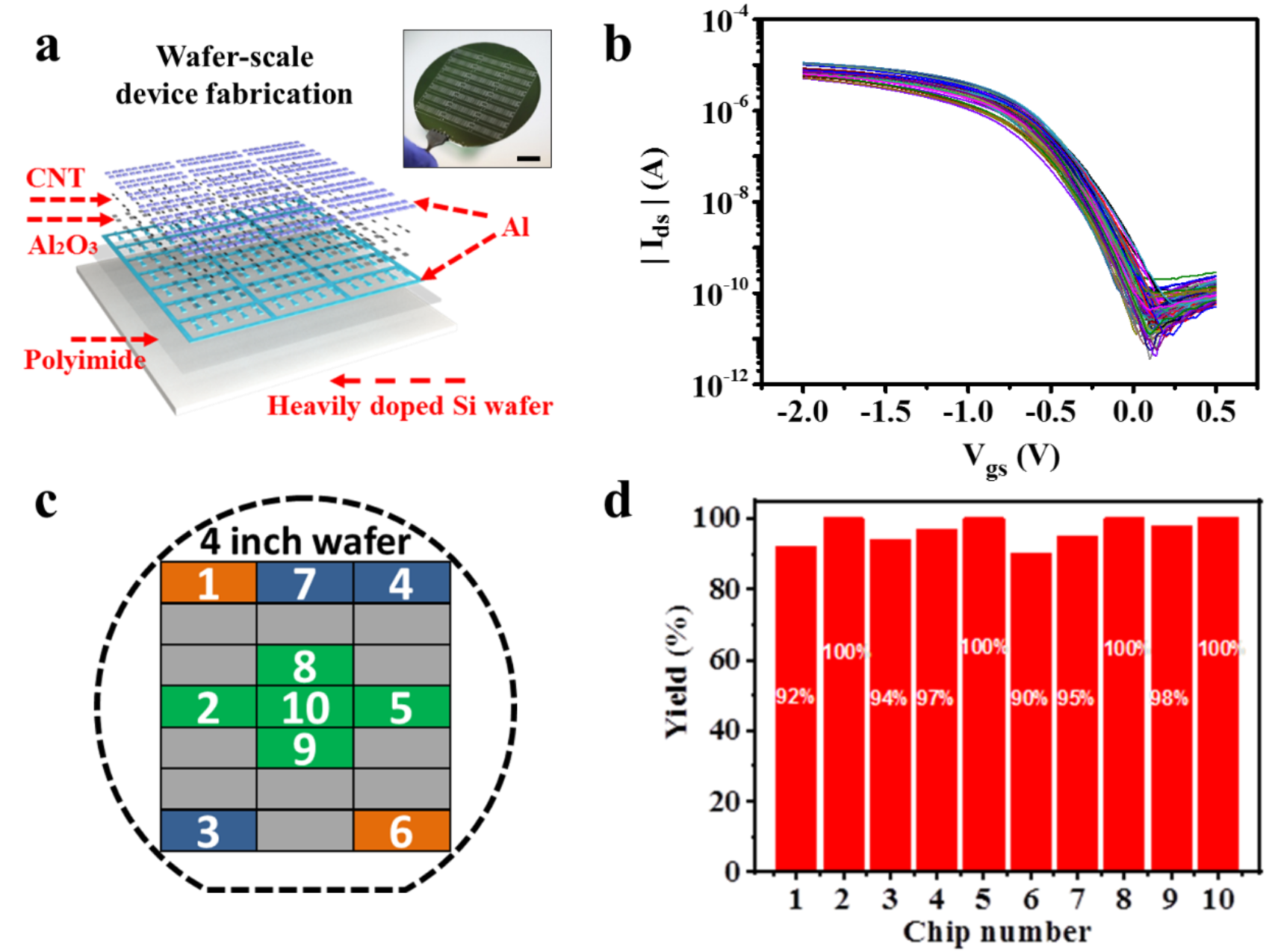
Recently, the research group of Hu Youfan, a key laboratory of the Department of Electronics and the Department of Physics and Chemistry of the Ministry of Education of the School of Information Science and Technology, Peking University, used the carbon nanotube network film as the channel material, and realized the wafer scale through transfer processing technology. Electronic components and integrated circuits that degrade themselves in the environment, have high yields and high uniformity, and in an artificial ecosystem, monitor and self-degrade environmental parameters.

Ad is: wafer size processing of the device; high uniformity of device performance obtained by processing; spatial distribution of device yield; device yield statistics of different chips
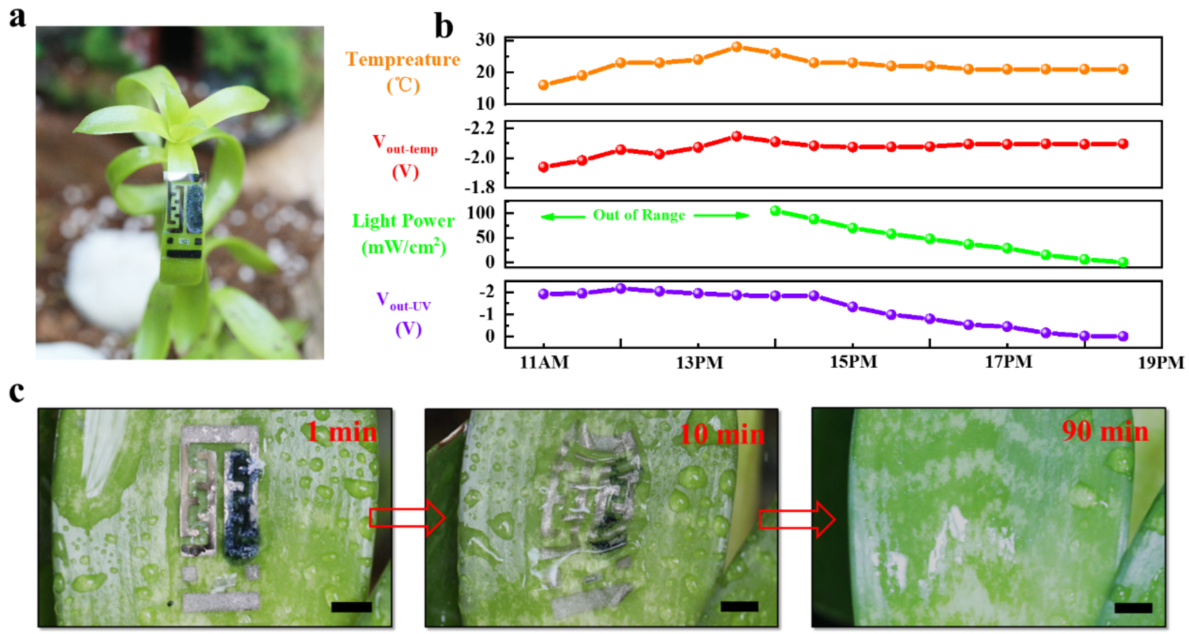
The research team fully utilized the advantages of the carbon tube low-temperature process to build basic electronic components and integrated circuits on the environmentally degradable flexible substrate to solve the problem of low yield of the transfer technology: on the one hand, the device was transferred to the target after processing The success rate of water-soluble substrates is as high as 100%; on the other hand, the average ratio of devices that can work properly is 96.6% in all devices. In addition, the prepared device has ultra-high uniformity, and the standard deviations of the transistor threshold voltage and the inverter transition voltage are 55 mV and 60 mV, respectively. A high-uniformity carbon nanotube transistor is used to prepare a basic logic gate (inverter, NAND gate, NOR gate) and a basic arithmetic unit (half adder) that can realize rail-to-rail output. They monitor the temperature and UV intensity near the surface of the plant in real time in an ecological chamber. After the monitoring is completed, the entire detection system can degrade itself under the action of artificial rain.

Ac is: sensing system on plant leaves; sensing system for real-time monitoring of light intensity and temperature in the environment; degradation of sensing system in artificial rain environment
Supported by the National Natural Science Foundation of China and the National Key Research and Development Program, the above results are based on "Wafer-scale high-yield manufacturing of degradable electronics for environmental monitoring". The title is published online in Advanced Functional Materials, 2019, 1905518, DOI: 10.1002/adfm.201905518. The 2015 Ph.D. student of the Department of Electronics is the first author, and Hu Youfan is the author of the communication. This series of results fully demonstrates the great advantages and application prospects of carbon nanotubes in high-uniformity, high yield, environmentally degradable transient circuits, and is expected to be used to build next-generation environmental monitoring platforms and the arrival of the Internet of Things era. Played a huge role in promoting.
Truck Camper Trailer
Truck Camper Trailer
Weifang Choice-link Trading Co., Ltd , https://www.ctraveltrailer.com